In the highly precise world of semiconductor chip wafer fabrication, Ultrapure Water (UPW) is an indisputable base. When chip nodes shrink to 5nm, 3nm and even beyond, trace contaminants could cause devastating problems, decrease yields and reduce the device’s reliability. The basis to this purity lies 18.2 MΩ·cm resistanceivity, which is the gold standard for water that is free of almost all particles, ions, organics and microbes. So what is the reason why 18.2 MΩ·cm ultrapure pure water is non-negotiable for wafer fabrication, what advanced RO and EDI systems provide this crucial resource and the tangible advantages it offers to modern manufacturing facilities.
18.2 MΩ·cm Is the Gold Standard for Chip Production
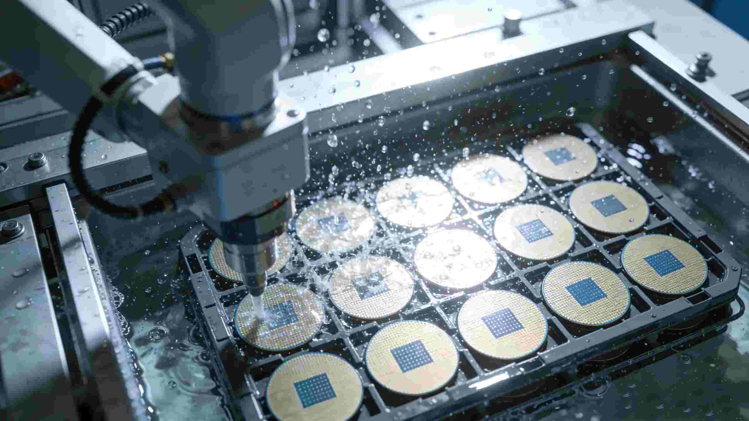
The semiconductor manufacturing process functions at a nanoscale level because any contamination exceeds 0.05μm or shows ionic levels of more than parts-per-billion will destroy an entire wafer. 18.2 MΩ·cm (at 25°C) is the theoretical peak of water purity, indicating zero measurable dissolved ions—the primary cause of electrical failures in microcircuits. The exceptional purity of semiconductor-grade ultrapure water meets SEMI F63 and ASTM D5127 standards.
Water with lower quality impurities leaves conductive residues and causes micro-scratches when performing CMP and alters the rate of chemical etching, thereby decreasing yields by 1% in the critical processes. To ensure the highest quality 3nm EUV processes, the metal ions have to be controlled at <0.01 per ppb, which makes 18.2 MΩ·cm of water not only the best, but also a must. It is different from the tap water (0.005-0.05 MΩ·cm) or RO water that is basic (0.1-1.0 MΩ·cm). Only 18.2 MΩ·cm UPW can ensure that wafers stay in perfect condition throughout each manufacturing stage.
Water Purity Levels Comparison for Chip Fabrication
| Water Type | Resistivity (MΩ·cm) | TOC (ppb) | Metal Ions (ppb) | Particles (>0.05μm) | Applicability in Chip Fabrication |
| Tap Water | 0.005–0.05 | >1000 | >1000 | >1000/mL | Not applicable (contaminant-heavy) |
| Basic RO Water | 0.1–1.0 | 50–100 | 10–50 | 10–50/mL | Low-end electronics (not wafers) |
| High-Purity Water | 10–15 | 5–10 | 1–5 | 1–5/mL | Mid-range electronics (not advanced chips) |
| Ultrapure Water | 18.2 | <1 | <0.01 | <1/mL | Semiconductor wafer fabrication (5nm/3nm/12-inch wafers) |
Key Role of Ultrapure Water in Wafer Fabrication Processes
Ultrapure water is a part of 80% of the manufacturing processes for chips, which is vital to the process in wafer cleaning, polishing, and the process of lithography.
Wafer Cleaning & Wet Etching
The most important use is post-etch rinsing that strips of chemical residues and particles, without leaving film. Pre-diffusion cleaning eliminates organic contaminants prior to high-temperature processing, and prevents dopant anomalies. Impurities in this process can cause irregular doping or short circuits, which are major causes of loss in yield.
Chemical Mechanical Planarization (CMP)
CMP creates an atomically smooth surface on wafers that is crucial for stacking chips in multi-layers. UPW creates uniform slurries and removes abrasive particles during the process, and cleans wafers following CMP. Minor impurities can result in cracks or uneven planearization damaging devices.
Photolithography & Advanced Processing
In the process of immersion lithography, UPW acts as the refractive medium used for EUV light, ensuring exact circuit patterning. It dilutes photoresists to exact concentrations and develops resists uniformly–contaminants blur features or create uneven layers. UPW can also chill high power lithography equipment in order to maintain thermal stability for the precision of nanometers.
Final Rinse & Quality Control
The final UPW rinse ensures zero residues before packaging. For 12-inch wafers, a single impurity can destroy hundreds of chips, making this step make-or-break for production efficiency.
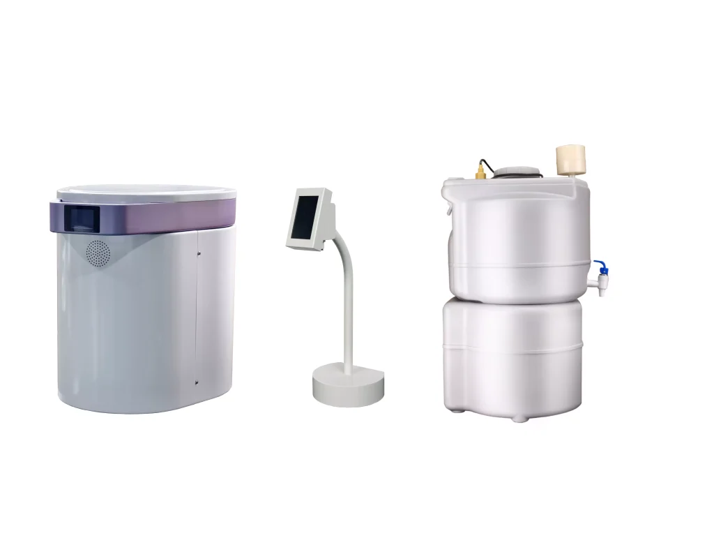
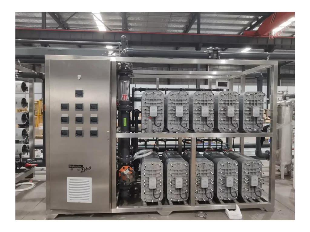
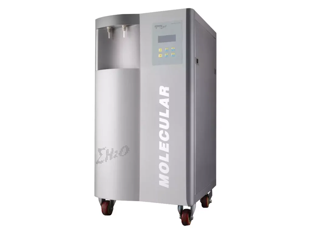
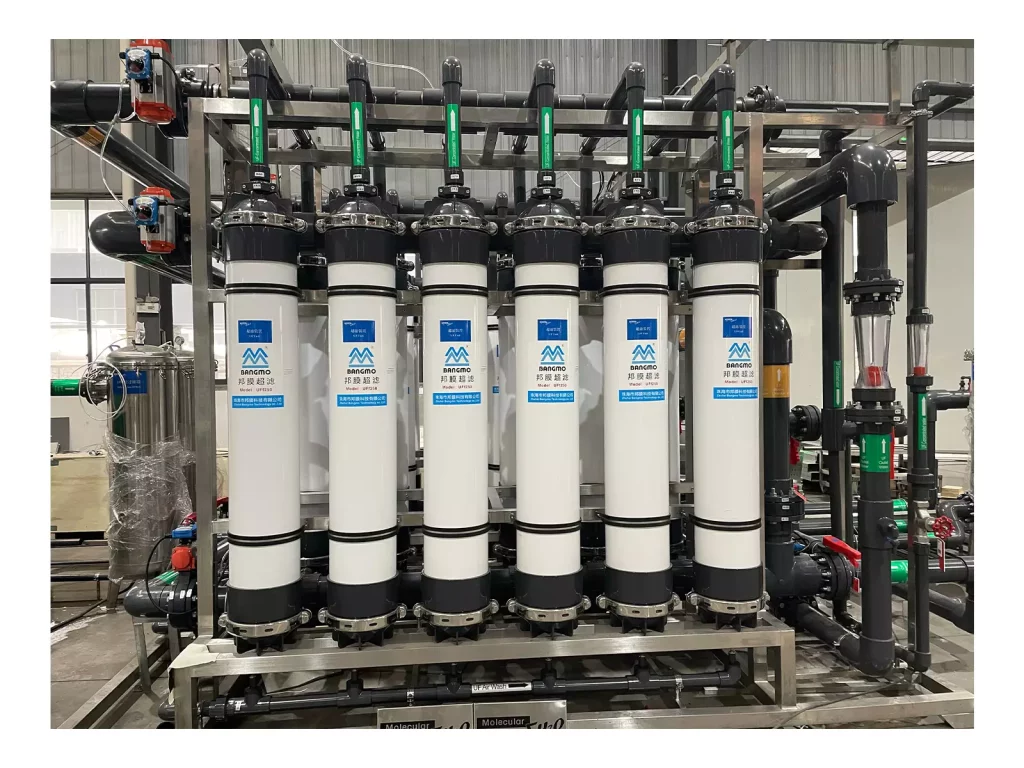
How RO + EDI Ultrapure Water Systems Work for Chip Fabrication
Achieving stable 18.2 MΩ·cm requires a multi-stage purification process—double-pass RO + EDI is the industry’s most reliable solution.
1. Multi-Stage Pretreatment
The system eliminates sediment and chlorine and large organic materials to ensure membrane protection for downstream operations. The activated carbon system functions together with multimedia filtration to prepare raw water for high-efficiency reverse osmosis system operation.
2. Double-Pass Reverse Osmosis (RO)
The first-pass reverse osmosis system removes between 97 and 99% of both dissolved solids and bacteria and endotoxins from the solution. The second-pass reverse osmosis system decreases ion concentrations which increases resistivity values to between 10 and 15 MΩ·cm and prepares water for EDI polishing.
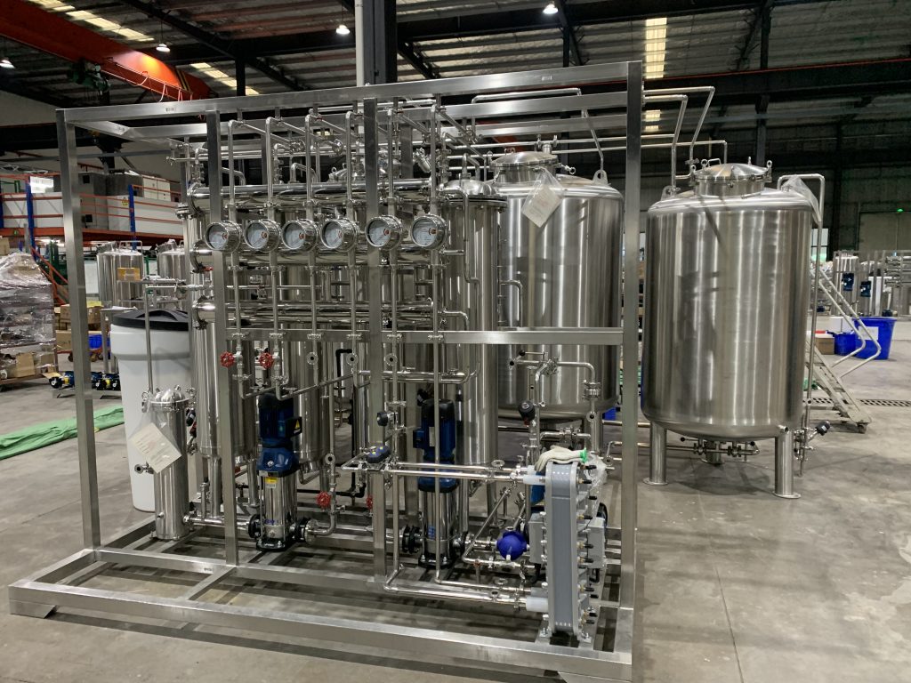
3. Electrodeionization (EDI)
EDI uses ion-exchange resins and electric fields to continuously remove residual ions without requiring any acid or alkali regeneration processes. The system processes material which produces an 18.2 MΩ·cm resistivity increase that maintains continuous operational purity throughout the entire day. EDI technology establishes operational efficiency by preventing chemical waste and production interruptions which occur in standard DI beds.
4. Final Polishing
The UV oxidation process operates at 185nm to decompose trace TOC until it reaches levels below 1 ppb. The water reaches SEMI standards through ultrafiltration at 0.05μm which eliminates micro-particles and through degasification which removes dissolved oxygen.
Core Advantages for Semiconductor Manufacturers
Unmatched Purity & Stability
RO and EDI systems provide continuous 18.2 MΩ·cm of continuous monitoring (resistivity TOC, particles, etc.). This stability prevents variations in batch sizes crucial for large-volume 24/7 fabrications.
Cost & Operational Efficiency
- Recuperation of water at high levels (up to 80-90%) reduces raw water consumption and also waste.
- The absence of chemical regeneration reduces O&M costs as well as safety risks.
- Fully automated and remote monitoring, it reduces the need for labor and downtime.
Compliance & Sustainability
Conforms to SEMI F63specifications, ASTM D5127, as well as ITRS specifications, which are the global specifications for manufacturing chips. Chemical-free EDI reduces carbon footprint and helps green fab goals.
Yield Improvement
Directly reduces defects from contamination, boosting yields by 3–7% for advanced nodes. High purity extends equipment life, lowering capital expenses.
Ideal Applications in Chip & Microelectronics Industry
- Semiconductor fabrication of wafers (5nm/3nm EUV, 12-inch wafers)
- Innovative IC packaging, as well as high density interconnects
- Microelectronics (sensors MEMS Power semiconductors, sensors)
- Flat panels and displays for photovoltaic cells
- Electronic materials and high-precision optics
In the process of chip wafer fabrication, 18.2 MΩ·cm ultrapure water isn’t just a luxury but essential. As semiconductor technology improves towards smaller nodes and increased complexity, the need for a flawless UPW increases. RO and EDI systems offer the ultra-pure, stable water fabs require to increase yields, assure device reliability and remain at the forefront of technology. For any semiconductor company striving for the highest quality by investing in a high-performance 18.2 MΩ·cm ultrapure system is the basis of successful operation.